The new breakthrough in semiconductor construction might be helpful to make electronic device get smaller. Researchers from the University of Chicago and Cornell University are united to develop a method of making silicon films that are only as thick as a few atoms, allowing them to be stacked on top of one another many times over. In this way, more powerful products might be produced ranging from personal electronic devices to solar-powered batteries. Nexteck Technology (7meditations.com, 400 882 8982, nexteck@nexteck.com) provides wide range of silicon related materials, such as Si sputtering target, Si evaporation materials, silicon wafer, silicon paste.

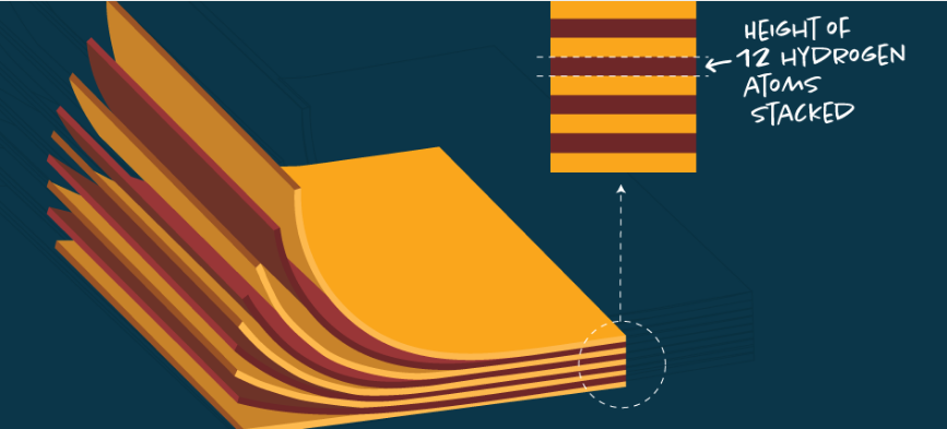
( Image source: UChicago Creative. )
Until now, these layers of silicon film were grown on top of one another, limiting the materials that they could be made with. The process of “growing” these layers requires materials that can withstand extremely high temperatures. This new method doesn’t require heat, as the layers are constructed individually and then laid down on top of one another. Instead of the layers being connected by strong covalent bonds, they’re connected with weaker bonds, allowing the integrity of their individual surfaces to remain intact.

( Image source: University of Chicago )
The ability to create layers of silicon films, atoms thick, may make it possible to shrink just about everything electronic. Imagine alternating layers of conductors and switches into three-dimensional electronic components or perhaps entire systems. Micro-machines could be included in the layers to provide sensors and actuators all on a single device. Without the need to drive signals off, chip power goes way down and performance goes way up. The possibilities are mind-boggling.
However, this method has its own defects. Putting atoms-thick layers down on top of one another precisely is challenging. Still, this innovative process may lead to countless breakthroughs in more fields of technology and industry than you can imagine.
( Article from : EET Taiwan )
Attending exhibitions, focusing on industry devolpment trend and new technologies,Nexteck Technology Limited keeps pace with the times ,exploring and innovating so as to achievingcontinous development.


